Summary:"Experience the Future: Students Explore MIT.nano's State-of-the-Art Cleanroom Facility"In a groundb
 referrerpolicy="no-referrer"
style="max-width:100%;height:auto;display:block;margin:0 auto;">
"Experience the Future: Students Explore MIT.nano's State-of-the-Art Cleanroom Facility"
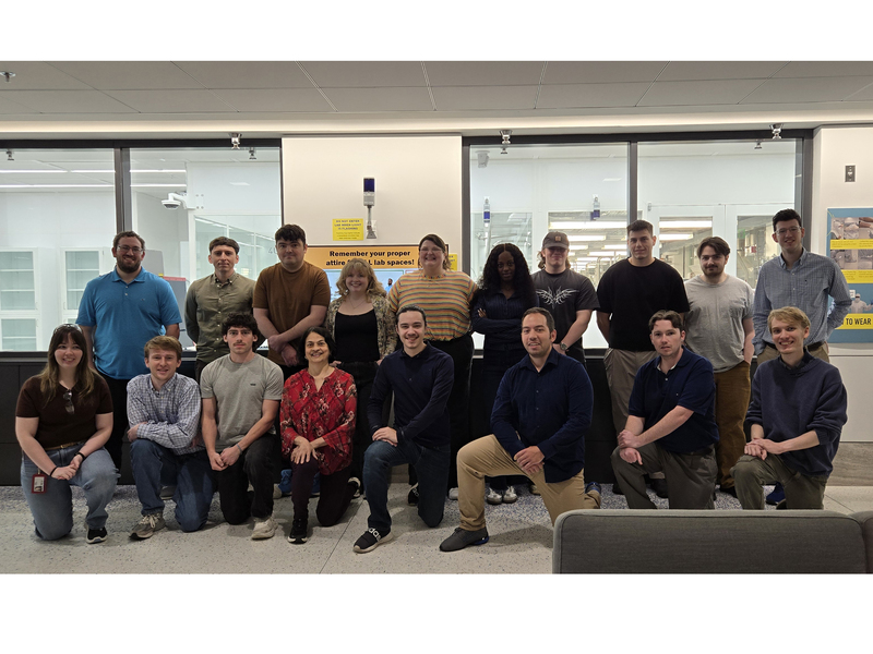
In a groundbreaking initiative, a select group of students recently had the opportunity to dive into the cutting-edge world of integrated photonics at the Massachusetts Institute of Technology's (MIT) nano-fabrication facility, MIT.nano. The hands-on boot camp, held at the Lab for Education and Application Prototypes (LEAP), marked a significant step forward in educating the next generation of engineers and researchers in the rapidly evolving field of photonics.
At the heart of this immersive experience was a comprehensive curriculum designed to equip students with the theoretical foundations and practical skills necessary to navigate the complexities of integrated photonics. Under the guidance of seasoned experts, participants spent several days working in the state-of-the-art cleanroom environment of LEAP, where they gained firsthand experience with the fabrication and characterization of photonic devices. This direct exposure not only deepened their understanding of the subject matter but also fostered a spirit of innovation and collaboration among the group.
The emphasis on integrated photonics reflects a broader industry trend towards the development of more sophisticated and efficient technologies. As the demand for faster data transmission rates and lower power consumption continues to escalate, the role of photonics in enabling these advancements is becoming increasingly pivotal. By providing students with access to world-class facilities and expertise, initiatives like the LEAP boot camp are playing a crucial role in shaping the future of this field.
Industry analysts point to the growing convergence of photonics and electronics as a key driver of innovation in the tech sector. As companies seek to leverage the benefits of integrated photonics in areas such as data communications and sensing, the need for skilled professionals with expertise in this area is expected to rise. Programs that offer hands-on training in state-of-the-art facilities are thus well-positioned to meet this demand, providing a critical link between academic theory and industrial practice.
Looking ahead, the success of the LEAP boot camp is likely to inspire further educational initiatives aimed at harnessing the potential of emerging technologies. As the boundaries between disciplines continue to blur, interdisciplinary programs that combine theoretical knowledge with practical experience will be essential in preparing the next generation of leaders in the tech industry. With its commitment to innovation and excellence, MIT.nano is set to remain at the forefront of this effort.
In conclusion, the MIT.nano LEAP boot camp represents a significant investment in the future of integrated photonics, providing students with a unique opportunity to engage with the latest technologies and techniques in a collaborative and supportive environment. As the industry continues to evolve, the impact of such initiatives is likely to be felt far beyond the walls of academia, driving innovation and shaping the technological landscape of tomorrow.