Summary:Revolutionary Breakthrough: Industry Leaders Smash 2D Transistor Scaling Barrier with Game-Changing
 referrerpolicy="no-referrer"
style="max-width:100%;height:auto;display:block;margin:0 auto;">
Revolutionary Breakthrough: Industry Leaders Smash 2D Transistor Scaling Barrier with Game-Changing Tech
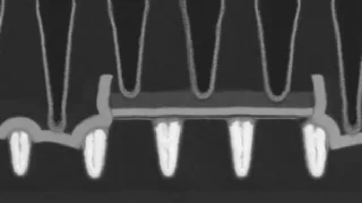
In a groundbreaking achievement, imec, ASML, and TSMC have successfully integrated both n-type and p-type transistors with atomically thin 2D channels on a single 300mm wafer, shattering the long-standing 2D transistor scaling barrier. This pioneering feat is poised to revolutionize the semiconductor industry, paving the way for the development of ultra-scaled transistors and next-generation electronics.
The collaborative effort has yielded a significant breakthrough, with the industry leaders demonstrating the co-integration of n-type and p-type field-effect transistors (FETs) using a 2D semiconductor material as the channel. By harnessing the potential of 2D materials, the consortium has overcome the limitations of traditional silicon-based transistors, enabling the creation of transistors with improved electrostatics and reduced leakage current. This development marks a significant milestone in the quest for transistor scaling, a crucial aspect of advancing semiconductor technology.
Industry analysts are abuzz with excitement, hailing this achievement as a game-changer for the semiconductor sector. The successful integration of 2D transistors on a 300mm wafer signifies a major step towards the adoption of 2D materials in mainstream semiconductor manufacturing. As the industry continues to push the boundaries of Moore's Law, this innovation is expected to play a pivotal role in driving the development of more powerful, efficient, and compact electronics. Moreover, the collaboration between imec, ASML, and TSMC underscores the importance of industry partnerships in driving technological advancements.
As the semiconductor landscape continues to evolve, the implications of this breakthrough are far-reaching. With the ability to fabricate ultra-scaled transistors, manufacturers can look forward to creating more sophisticated and powerful devices, from smartphones to datacenter processors. Furthermore, the integration of 2D transistors is expected to enable the development of novel applications, such as flexible electronics and neuromorphic computing.
In conclusion, the collaborative achievement by imec, ASML, and TSMC represents a seismic shift in the semiconductor industry, as it tackles one of the most pressing challenges in transistor scaling. As the industry continues to capitalize on this breakthrough, we can expect to witness the emergence of innovative technologies that will transform the electronics landscape. With this game-changing development, the future of semiconductor technology has never looked brighter.